Research
Research concept
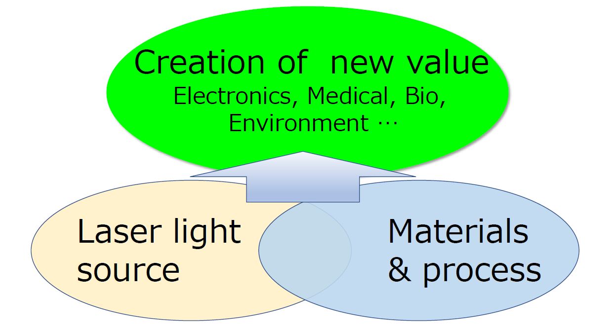
Our Innovative Laser Processing Group aims to develop frontier laser-based technologies, that create “New value” in major industrial fields such as electronics, manufacturing, medical, environmental, and biotechnology. Our group is a gathering of experts in the both fields of laser light sources and processing, leading to a real innovation. Dr. Narazaki is working on a variety of laser processes for a better future, such as material delivery by laser-induced transfer, laser microfabrication, laser-induced heat simulation based on finite element method and so forth.
Major topics
- Material delivery by laser-induced transfer
- Data-driven laser procedssing
- Ultrafast laser procedssing of ceramics
- Laser microfabrication of various materials and devices
- Laser surface modification
- Real-time measurements & simulation of laser processing
Details of each theme
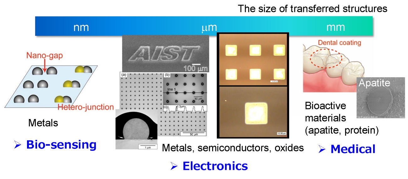
1. Material delivery by laser-induced transfer
Keywords: nano/micro dots, direct-write, protein, coating for early healing, electronics, medical applications
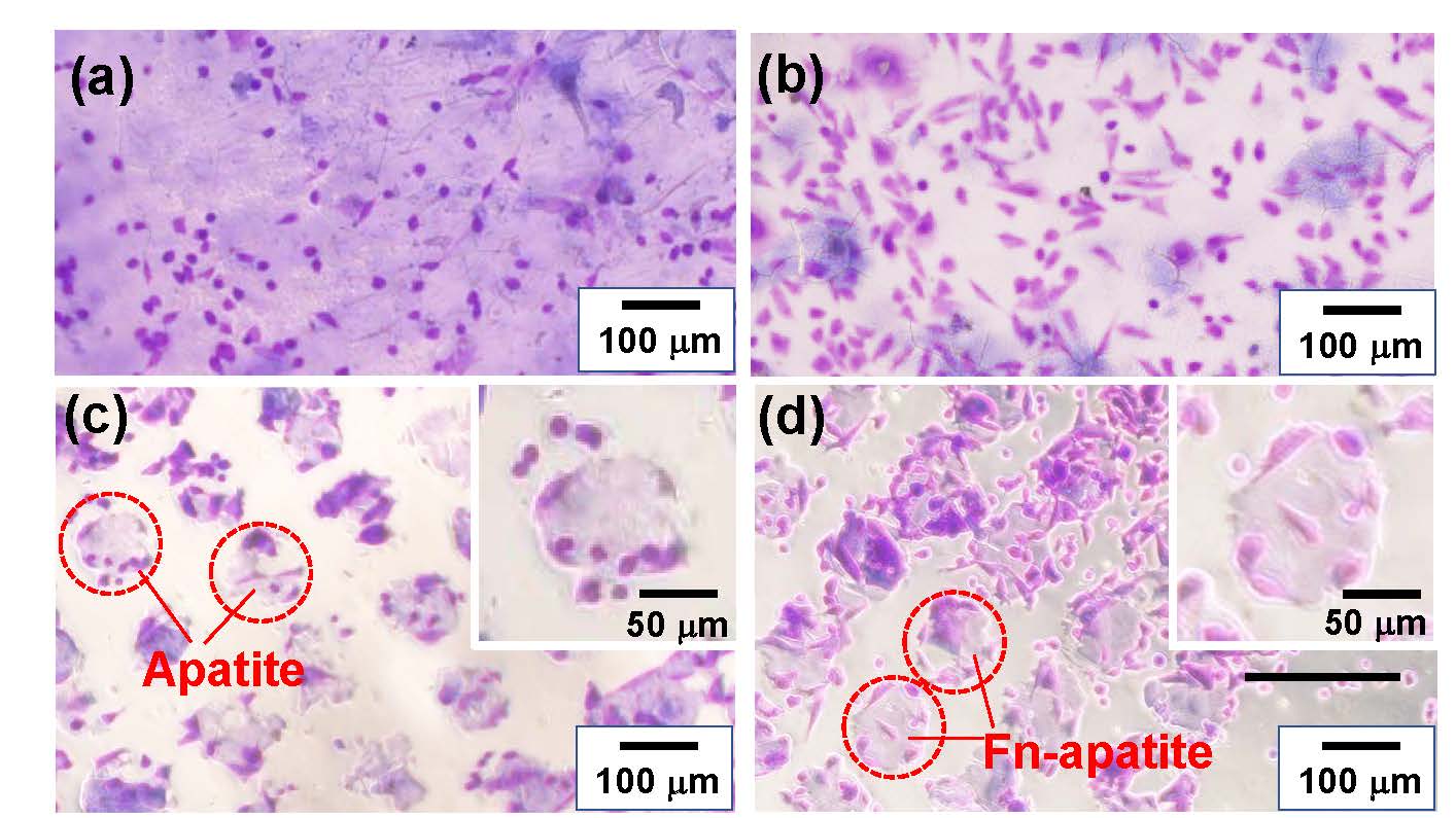
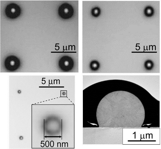
When pulsed laser light is irradiated on materials, laser ablation of the material is induced as a result of transient / local high-temperature and high-pressure. "Laser-induced transfer" is a method that utilizes the laser ablation to deliver substances. According to the laser-induced transfer, a wide range of substances such as nano / microparticles and even proteins can be deposited on demand.
We are currently working with researchers at other universities in order to explore how small nanoparticles can be deposited and how we can deliver with highly physiological-active protein by this method.
using laser-induced transfer.
References
- “Nanodot array deposition via single shot laser interference pattern using laser-induced forward transfer”, Yoshiki Nakata, Eiki Hayashi, Koji Tsubakimoto, Noriaki Miyanaga, Aiko Narazaki, Tatsuya Shoji, and Yasuyuki Tsuboi, International Journal of Extreme Manufacturing, (2020) in press; https://iopscience.iop.org/article/10.1088/2631-7990/ab88bf/pdf.
- “Bioactive micropatterning of apatite immobilizing cell adhesion protein by laser-induced forward transfer with a shock absorber”, Aiko Narazaki, Ayako Oyane, Saki Komuro, Ryozo Kurosaki, Tomoko Kameyama, Ikuko Sakamaki, Hiroko Araki, and Hirofumi Miyaji, Optical Materials Express, 9 (2019) 2807; https://doi.org/10.1364/OME.9.002807.
- "On-Demand Patterning of Indium Tin Oxide Microdots by Laser-Induced Dot Transfer",A. Narazaki, R. Kurosaki, T. Sato, and H. Niino, Applied Physics Express,6 (2013) 92601.
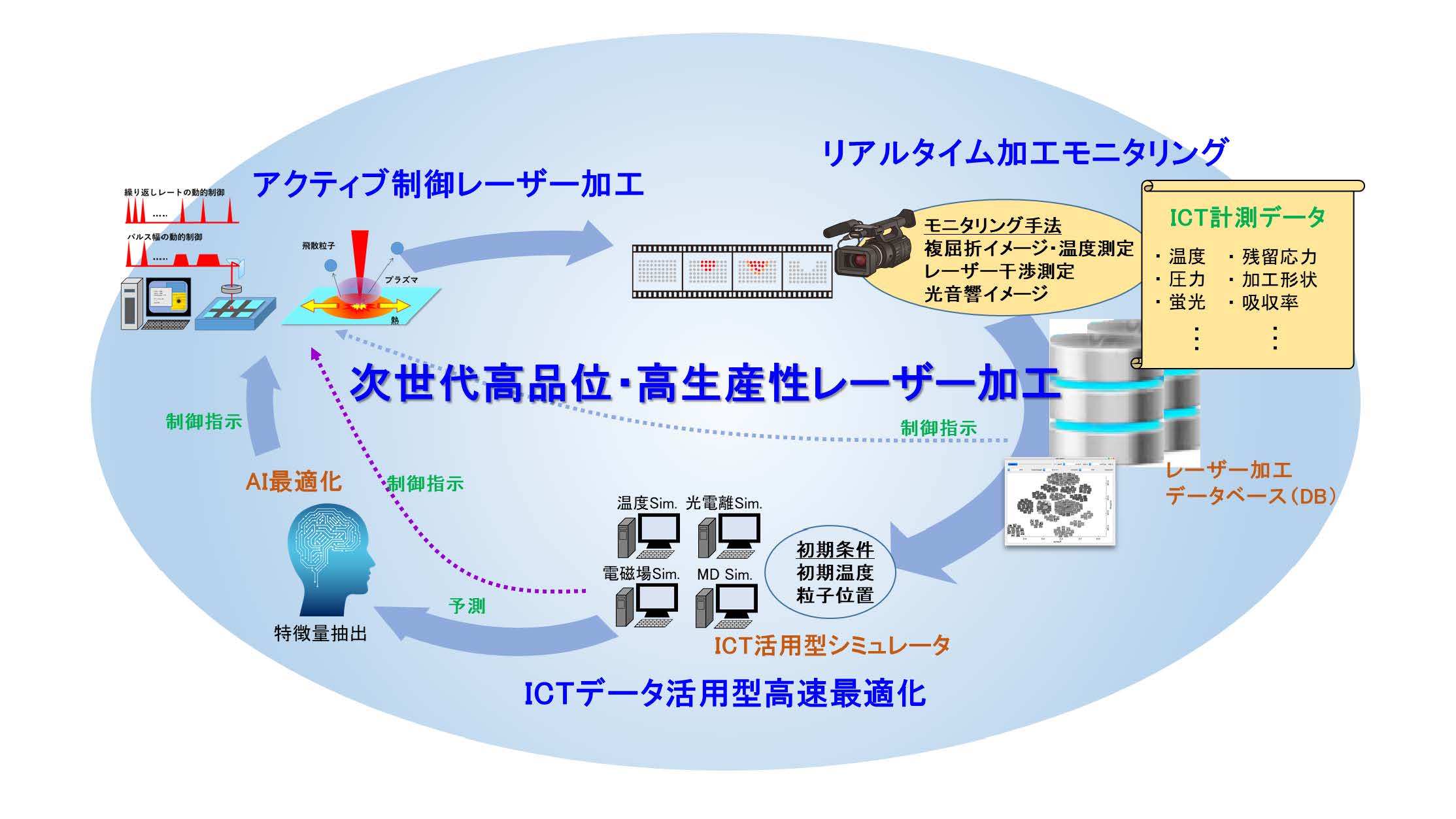
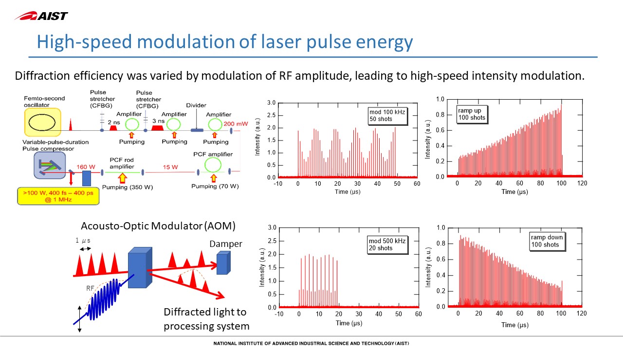
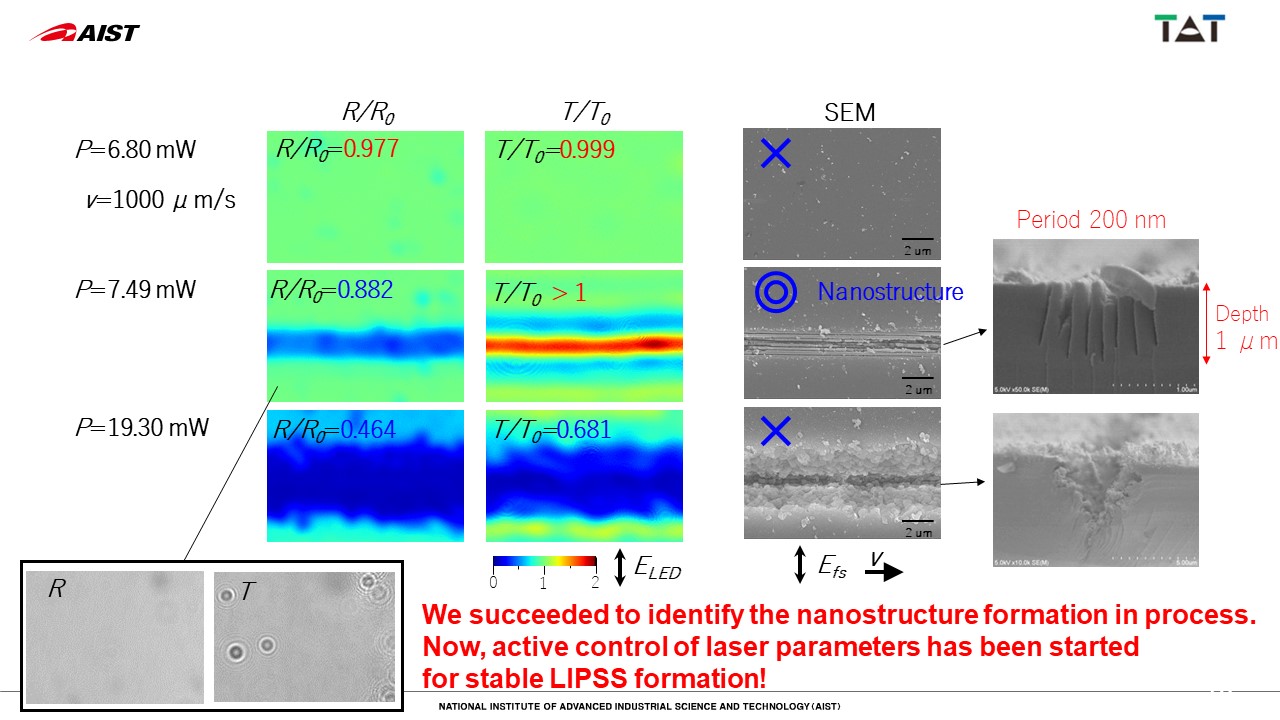
2.Data-driven laser processing
Keywords: Parameter optimization, In-process monitoring, AI, Simulator, Active laser control, Laser-induced periodic surface structures (LIPSS), Glass, Transparent materials
For industrial implementation of advanced laser processing, it is important to quickly optimize multi-parameters. Until now, process optimization has relied on the experience and intuition of engineers, but in order to strengthen industrial competitiveness and save labor, there is a strong demand for the system that can optimize with less time- and labor-consuming. Therefore, through R&D of core technologies such as in-process monitoring, AI that achieves high-speed optimization from the data, and ultra-high-speed laser control ("Active laser control") that quickly responds to optimization parameters, we are working on the development of data-driven laser processing. Recently we demonstrated the LIPSS formation on glass with a remarkable improvement in yield by integration of our core technologies such as in-process monitoring and feed-back control of laser intensity.
References
- “Data-driven ultrashort pulse laser processing toward real-time CPS”, A. Narazaki, D. Yoshitomi, H. Takada, D. Nagai, G. Miyaji, ICALEO 2022 Proc, Micro701 (2022) 1-6.
- "In-process monitoring of femtosecond laser-induced periodic nanostructures on glass by using anti-reflective property", D. Nagai, H. Takada, A. Narazaki, G. Miyaji, Proc of SPIE Laser Applications in Microelectronic and Optoelectronic Manufacturing (LAMOM) XXVIII, 12408 (2022) 124080O.
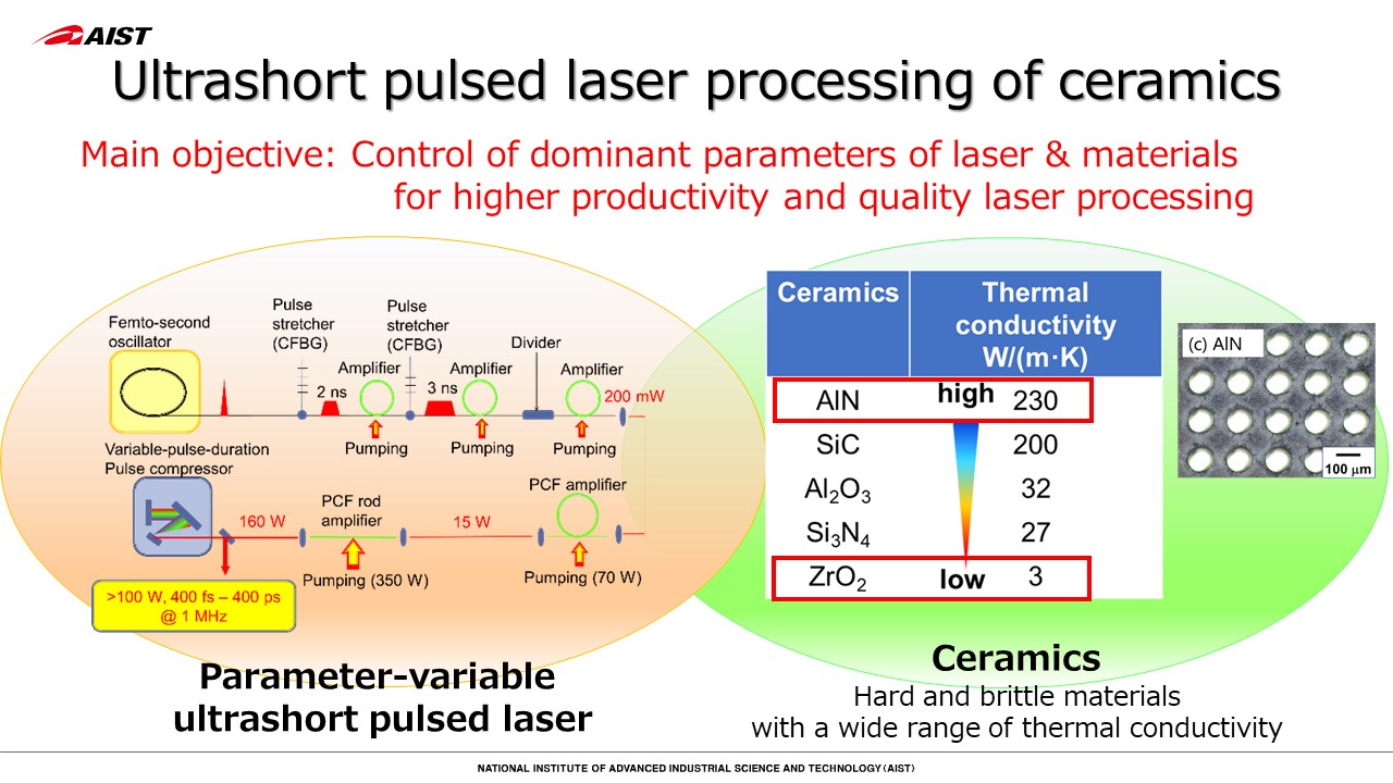
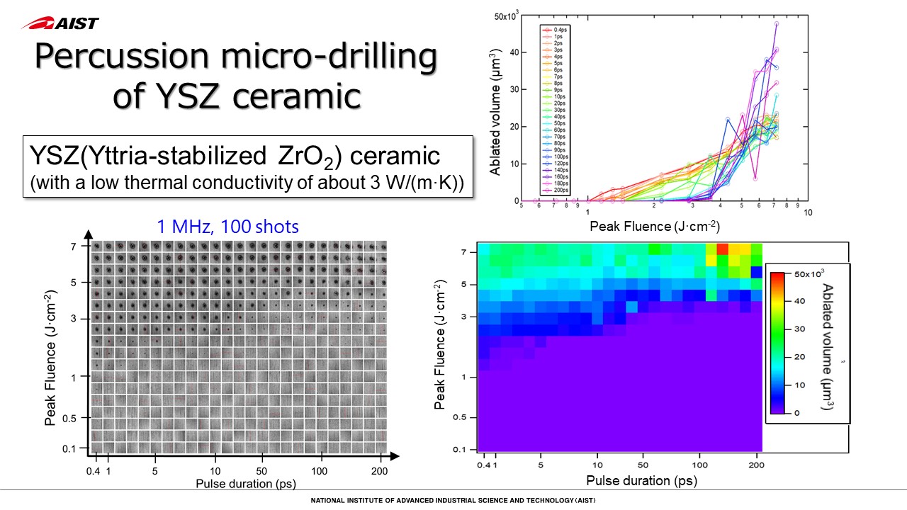
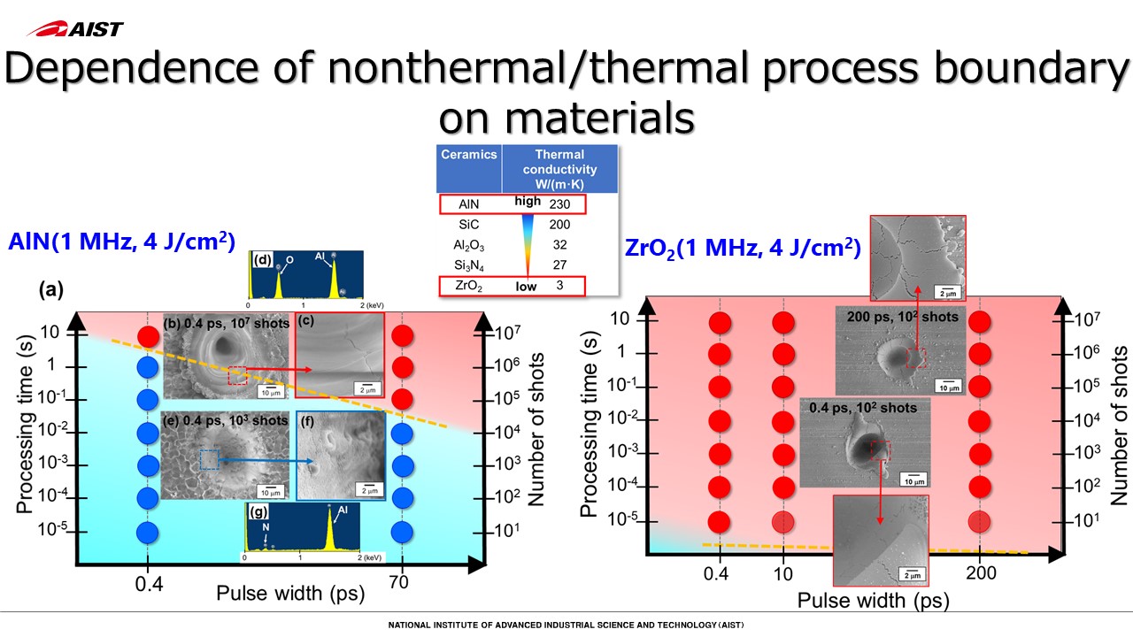
3.Ultrafast laser procedssing of ceramics
Keywords: ultrafast laser, ceramics, micro-hole drilling, cutting, AlN, Al2O3, YSZ, CMC
Currently participating in the NEDO project on the development of high brightness and efficiency next generation laser technology, we are developing laser light sources , that can vary parameters over a wider range comparing with conventional light sources, and innovative laser processing using our new lasers. Using this laser system, we have investigated nonthermal-thermal laser processing boundaries for various ceramics.
References
- “Study on nonthermal–thermal processing boundary in drilling of ceramics using ultrashort pulse laser system with variable parameters over a wide range”, Aiko Narazaki, Hideyuki Takada, Dai Yoshitomi, Kenji Torizuka, and Yohei Kobayashi, Applied Physics A, 126 (2020) 252; https://link.springer.com/article/10.1007/s00339-020-3410-2.
- “Pulse Width Dependence of Heat Accumulation in Ultrashort Pulse Laser Processing”, Aiko Narazaki, Hideyuki Takada, Dai Yoshitomi, Kenji Torizuka, and Yohei Kobayashi, ICALEO 2019 Proceedings, (2019) Nano604.
4.Laser microfabrication of various materials and devices
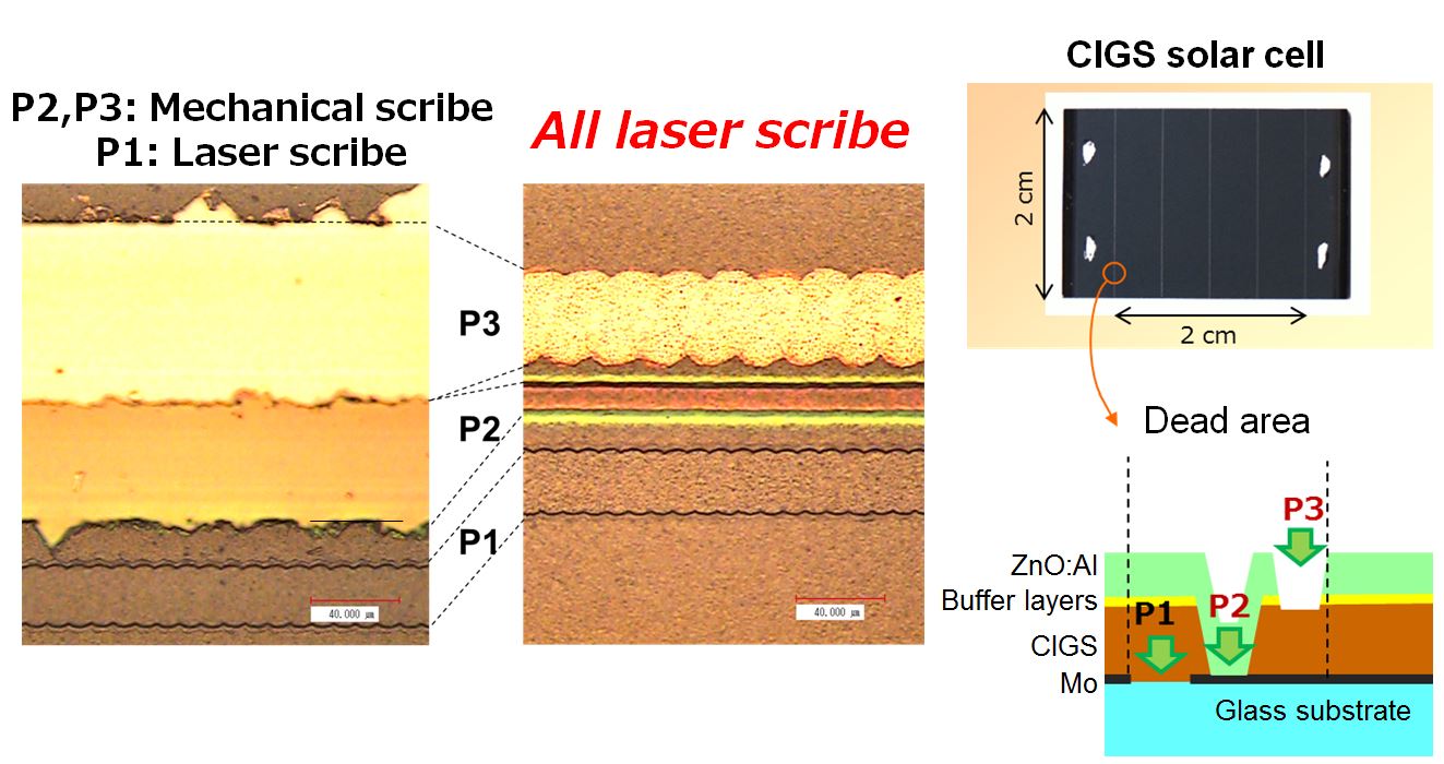
Keywords: glass, semiconductor, hole drilling, CIGS thin-film solar cell, laser scribe, transparent conductive oxide (TCO)
Laser processing market is expanding on a global scale because the laser processing has become one of essential tools in manufacturing industry. To date, we have demonstrated surface microfabrication of various materials like glasses, ceramics, semiconductors.
Further, by taking advantage of the diversity of research fields in AIST, we have developed laser processing and characterization technologies of semiconductor devices such as a highly-efficient CIGS thin-film solar cells.
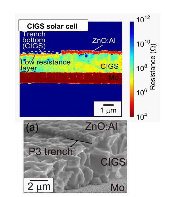
by TCO lift-off: (Up) a cross-sectional mapping
of electrical resistance and (Down) a SEM image
of the laser-scribed groove.
References
- “Evaluation of femtosecond laser-scribed Cu(In,Ga)Se2 solar cells using scanning spreading resistance microscopy”, Aiko Narazaki, Jiro Nishinaga, Hideyuki Takada, Tadatake Sato, Hiroyuki Niino, Kenji Torizuka, Yukiko Kamikawa-Shimizu, Shogo Ishizuka, Hajime Shibata, and Shigeru Niki, Applied Physics Express, 11 (2018) 032301.
- “Fabrication of Micropits by LIBWE for Laser Marking of Glass Materials”, Tadatake Sato, Aiko Narazaki, and Hiroyuki Niino, Journal of Laser Micro / Nanoengineering, 12 (2017) 248-253.
5.Laser surface modification
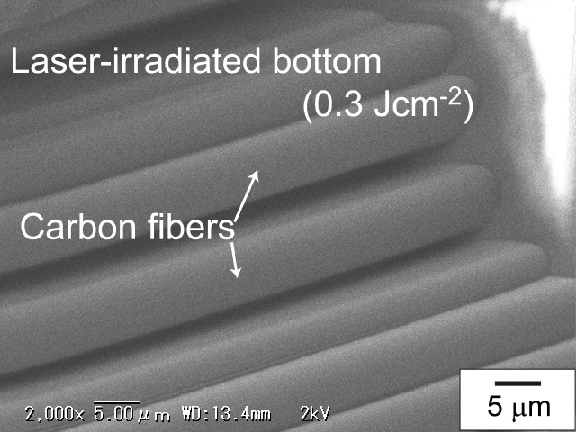
Keywords: CFRP, laser cleaning, TiO2-contained glass, photocatalytic property, micro-channel
Surface modification is a key technology since a material surface largely affects the functionality, durability and designability of materials. So far, we have demonstrated the surface modification of carbon fiber reinforced plastics (CFRP) and multi-components glasses. These are not only useful for industries, but also as "unique phenomena" reflecting the difference in light and thermal characteristics between multiple components.
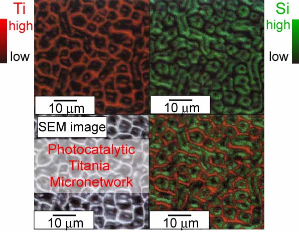
for TiO2-SiO2 glasses by ns UV laser irradiation.
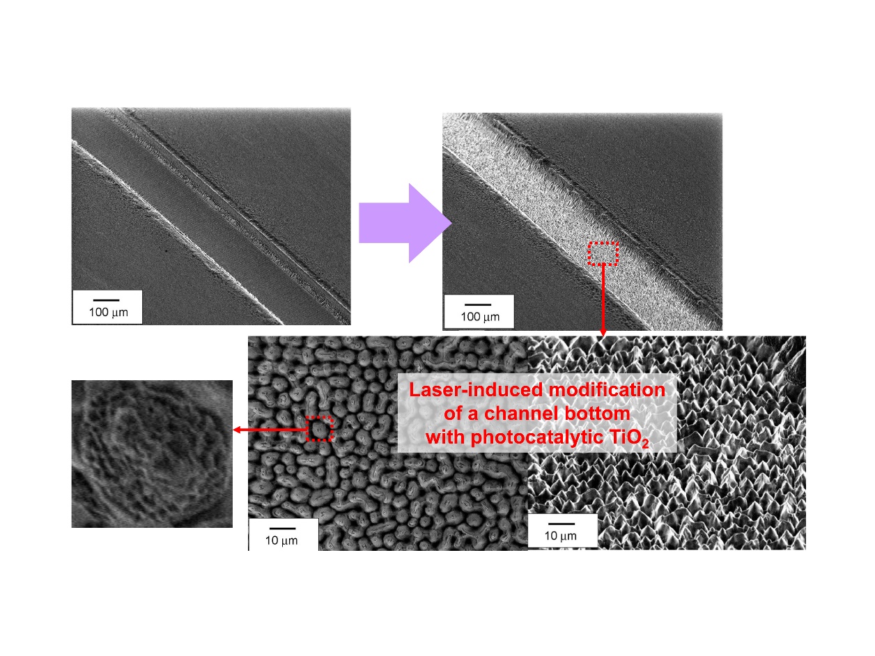
and laser-induced modification of a channel bottom with photocatalytic TiO2.
References
- "Laser Ablation of Carbon Fiber Reinforced Plastics: Laser-Ionization TOF Mass Spectrometric Study",A. Narazaki, T. Sato, Y. Kawaguchi, and H. Niino, Journal of Laser Micro / Nanoengineering,9 (2014) 59.
- "Formation of a TiO2 micro-network on a UV-absorbing SiO2-based glass surface by excimer laser irradiation",A. Narazaki, Y. Kawaguchi, H. Niino, M. Shojiya, H. Koyo, K. Tsunetomo,Chemistry of Materials,17 (2005) 6651.
6. Real-time measurements & simulation of laser processing
Keywords: Finite element method (FEM) simulation and sensing of laser processes
In order to further improvement on the quality and throughput of laser processing, it is important to measure and visualize of the processing.
We have visualized shock waves and bubble generation in the LIBWE by shadow graph method. In addition, we have visualized the state of transient high temperature distribution in raw material during laser-induced transfer by heat transfer simulation using finite element method, examined the mechanism, and utilized it for parameter optimization.
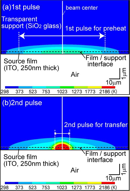
for double-pulse LIFT.
References
- "On-Demand Patterning of Indium Tin Oxide Microdots by Laser-Induced Dot Transfer",A. Narazaki, R. Kurosaki, T. Sato, and H. Niino, Applied Physics Express,6 (2013) 92601.
- “Transient pressure induced by laser ablation of toluene liquid: toward the understanding of laser-induced backside wet etching”,Y. Kawaguchi, X. Ding, A. Narazaki, T. Sato, and H. Niino, Applied Physics A-Materials Science & Processing,79 (2004) 883.